
| Project of the Month - January 2011
SEMIDEC is an ambitious Support Action project aimed at stimulating cooperation in the design of semiconductor components and electronic based miniaturised systems between Europe and Russia, in order to support Europe’s leading position in integrated circuit product innovation. Consequently, SEMIDEC aims to develop cooperation in semiconductor design methods and tools that are relevant to the research priorities identified in the FP7 ICT Work Programme 2009 and ENIAC Strategic Research Agenda 2007.
These research priorities include the following:
In order to stimulate the semiconductor design cooperation, SEMIDEC ’s mission is threefold:
The figure below provides an overview of the European and Russian partners involved in SEMIDEC.
The SEMIDEC team has recently published a promotion guide for Russian semiconductor organisations; major report about Russian semiconductor research, technology and organisations; and good practice booklet for FP7 semiconductor design research. All three publications can be found here.
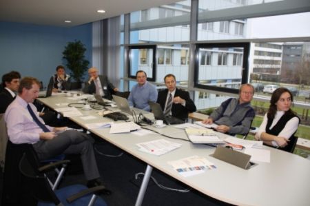
In September, the SEMIDEC project recently held a successful workshop at St Petersburg State Polytechnical University. The workshop attracted distinguished microelectronics experts from industry and academia from France, Germany, Russia, Spain and Sweden. As an encouraging result of the workshop, detailed discussions have been started on preparation of FP7 research proposals involving Russian partners and secondment of Russian researchers in Europe.
Giles Brandon, Intelligentsia
Project coordinator
gilesbrandon@intelligentsia-consultants.com
Prof. Alexander S. Korotkov, St Petersburg Polytechnical University
Russian Scientific Leader
korotkov@rphf.spbstu.ru
Johann HAUER, Fraunhofer-IIS
European Scientific Leader
johann.hauer@iis.fraunhofer.de

This external link opens a new window:
(URL: http://semidec-ru.eu/)